|
Nanoelectronics
Research Lab |
|
||||||
|
Rotationally
Controlled van der Waals Heterosturctures
The
isolation of graphene, a two-dimensional (2D) layer of carbon in 2004, and
subsequently of other materials such hexagonal boron-nitride and transition
metal dichalcogenide have opened up an entire new
world of possibilities to design and realize van der Waals heterostructures, to create quantum materials with
entirely new properties. A key ingredient that can add a new dimension to the
atomic layer heterostructures palette is the
rotational control, and alignment of different 2D layers. We are interested
in developing new techniques to realize rotationally controlled van der Waals
heterostructures of 2D materials, and to explore
quantum transport and device applications of these materials. Below are two examples from our current
research.
Controlled
Moiré Patterns of 2D Materials
Moiré
patterns created by stacking van der Waals materials have opened up new
opportunities to band engineering and collective quantum states in
two-dimensional materials. At certain twist angles between the two layers,
electrons can move with very low velocity, which stabilizes collective states
such as superconductivity. We are investigating the exciting new physics of
interacting electrons in these systems.
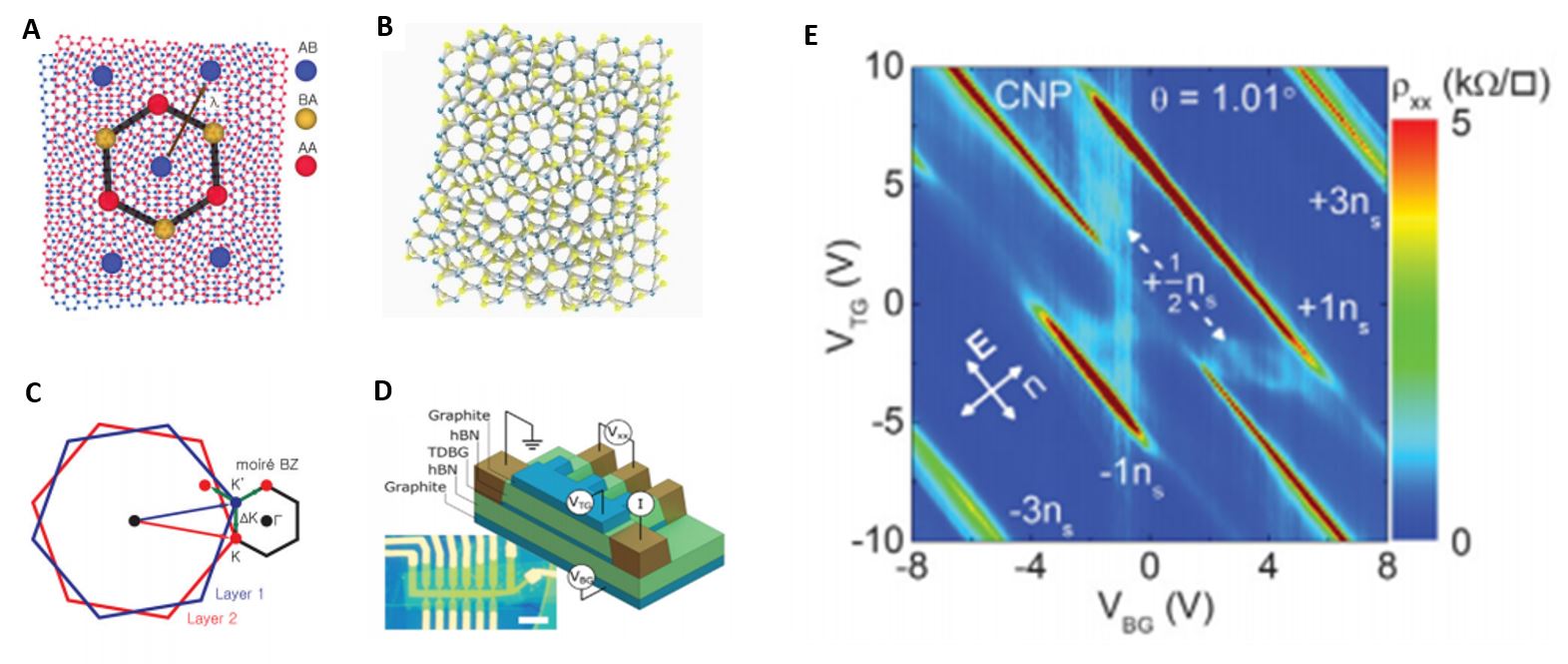
(A) Illustration of the local stacking in
twisted bilayer graphene. (B) Schematic of a twisted TMD bilayer. (C) The
first Brillouin zone (BZ) of each graphene layer (red, blue) in twisted
bilayer graphene, along with the BZ (black) of the moiré pattern. (D) Optical
micrograph and schematic of the Hall bar used to probe transport in a moiré pattern realized in twisted double
bilayer graphene. (E) Contour plot of the resistance vs. top and bottom gate
bias in a dual-gated twisted double bilayer graphene. Resistance maxima are observed at integer, and fractional moiré band filling
factor. Resonant
Tunneling and Exciton Condensates in Double Layers
of 2D Materials
Collective
quantum states can form when two layers of electrons or holes are brought in close proximity. One example consists of
two graphene layers separated by a thin tunneling barrier. When the two graphene
layers are tuned to equal and opposite charge densities, electrons in one
layer can bind with holes in the opposite layer to form indirect excitons, which may condense at low temperatures. We have
developed exquisite techniques to fabricate twist-controlled double layers of
graphene or transition metal dichalcogenides with
independent contacts to each layer.
The tunneling current-voltage characteristics between the two layers
can serve as a powerful tool to probe energy and momentum tunneling, as well
as many-body enhanced tunneling and other signatures of exciton
condensates.
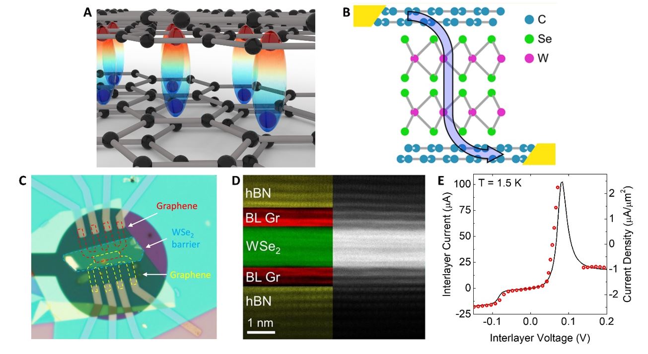
A) Illustration showing pairing of electrons
and holes in separate graphene bilayers to form indirect excitons.
(B) Schematic of the tunneling between two graphene bilayers separated by a
WSe2 barrier. (C) Optical micrograph showing a graphene – Wse2
– graphene tunneling heterostructure encapsulated
in hBN. (D) Transmission electron microscope image
showing the individual atomic layers in a tunneling heterostructure.
(E) Tunneling characteristic showing negative differential resistance. Growth
of Germanium, Silicon Nanowires and Core-Shell Heterostructures
Semiconductor
nanowires offer a natural, quasi-one dimensional test-bed for electron
physics in reduced dimensions and as a
platform for electronic devices. Core-shell nanowires represent the quasi
one-dimensional counterpart to the two-dimensional quantum well. We are
exploring the growth of band- and strain-engineered Ge-SiGe and Si-SiGe
core-shell nanowires in order to tailor the structure’s electronic
properties. We have also grown modulation doped Ge-SiGe nanowires as a method
to enhance the carrier mobility of this system.
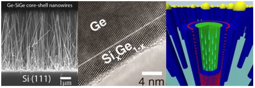
Electron microscope images of core-shell nanowires
and cut-away schematic of modulation doped core-shell nanowire |
|||||
Last update 1/17/2020